Functional Materials Laboratory (Yasutake Laboratory)
|
“Novel Functional Materials – key to the future technology”
For the progress of advanced technology and basic science, it is essential to improve the performance of functional materials, and also to create materials with completely new functions. In addition, commercialization of the functional materials requires a production technology that is highly efficient as well as friendly to humans and the environment. Our laboratory is conducting researches in the following fields: (1) development of new Earth-conscious technologies for the formation of high-performance functional thin films, (2) creation of novel functional materials of which surface, interface and bulk properties are controlled at atomic level, and (3) fabrication of highly functional thin films and their application to actual electronic devices. Our current research projects include: (1) development of low-temperature, high-rate, high-performance, and ecoclean film formation technologies, which take advantage of the physical and chemical properties of atmospheric-pressure very high-frequency (VHF) plasma, and (2) application of the functional thin films to high-performance solar cells, thin film transistors, high-sensitivity sensors, and devices with new functions.
Development of atmospheric-pressure plasma CVD (AP-PCVD) realizing high-rate and low-temperature deposition of high-quality functional thin films
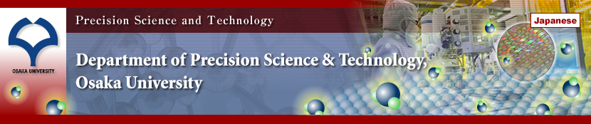
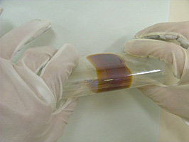
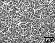
Atmospheric-pressure VHF plasma is a new type of plasma with a high radical density and small ion energy. This research project utilizes these characteristics to develop a technology for the high-rate and low-temperature fabrication process of high-quality semiconductor thin films. Figure 1 shows a single-crystal pure silicon (Si) thin film without crystallographic defects, which has been prepared at a high rate and at a temperature that is more than 500°C lower than conventional methods, together with a photograph of the atmospheric-pressure plasma used in this process.
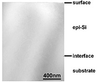
<Figure 1>
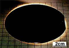
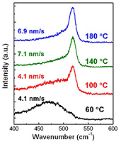
Low-temperature and high-rate fabrication process of thin films for flexible electronic devices
Film-based electronics is one of the prime candidates for the electronics industries in the future. To realize this, we are studying a technology to form Si-related thin films at high rates and at low temperatures close to room temperature. Figure 2 shows an example of the low-temperature and high-rate deposition of a microcrystalline Si (µc-Si:H) film. The figure clearly demonstrates that we can fabricate a µc-Si:H film at a low temperature of 100°C. Thus, it is possible to use a plastic film, which has a low heat resistance, as a substrate. We aim to apply this technology to the production of highly functional devices, such as flexible displays and film type sensors.
 ↑ Zoom |
 |
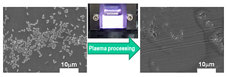
Development of atmospheric-pressure plasma-enhanced chemical transport (APECT)
The atmospheric-pressure plasma-enhanced chemical transport is a new atmospheric-pressure plasma technology that is capable of forming and etching functional materials. In the APECT process, we do not use any toxic and pyrophoric source gases, such as SiH4, B2H6, GeH4, CF4, but use safe and easy-to-handle solid materials. Currently, using this technology, we are developing a highly efficient method to form functional thin films of polycrystalline Si, SiGe, SiC, etc., which are expected to be used in thin film solar cells. Moreover, we are aiming to realize etching processes of Si and its alloys that do not use any global warming gases. Figure 3 shows electron micrographs of selectively grown Si films (a and b) and a carbon nanofiber (c) fabricated by APECT.
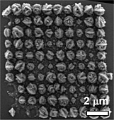
<Figure 3>
Application of mist-mixed atmospheric-pressure plasma to bio- and agriprocesses
This project aims to develop a surface processing technology that combines the features of “atmospheric pressure” and “plasma”, which is applicable to medical care, food industries, and agriculture industries. Figure 4 shows an example of room temperature sterilization. The supply of liquid source material (water) to the atmospheric-pressure plasma in mist form (microscopic liquid particles) results in the efficient generation of reactive molecules in the plasma. The figure clearly indicates that the live bacteria (Bacillus subtilis) are deformed due to the chemical reactions with the reactive molecules.
<Figure 4>
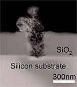
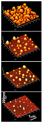
Ge nanostructure
The process of thin film growth depends on the condition of the substrate surface. Therefore, it is possible to produce thin film materials with superior properties by improving and controlling the surface condition of the substrate. Figure 5 shows an example of fabricated germanium nanocrystals, which can be used as the nuclei for the crystalline silicon growth on a glass substrate. We have employed the newly developed oxygen etching process to control the diameter and density of germanium nano-crystals.
565-0871, Japan
Department of Precision Science & Technology, Osaka University
E-mail:
www_admin[at]prec.eng.osaka-u.ac.jp