nanoManufacturing Science Laboratory (Yamamura Laboratory)
|
Jump to nanoManufacturing Science Laboratory 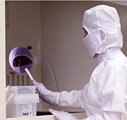 |
Ultra-micro devices with new functions to support the information revolution
New high-performance devices where each electron is precisely controlled are needed to develop the next generation of supercomputers and future multimedia technology. To realize these future technologies, our laboratory makes extensive use of advanced equipment to create ultra-micro structures where the arrangement of atoms is precisely controlled. These ultra-micro structures can be used to fabricate micro-devices with new functions by controlling the electrons. In addition, high-performance devices, which are realized by integrating these micro devices with new functions, will enable huge quantities of information to be processed and global ultra-high speed communication. Thus, these devices will contribute to vitalizing our modern culture and creating new industries. Hence, ultimately advanced equipment systems which create ultra-micro structures and devices with new functions will connect humans to the world of atoms and electrons, thereby pioneering an affluent future.
Our laboratory is currently working on research projects such as (1) development of ultra-microfabrication on semiconductor surfaces in an ultra-clean environment, (2) exploration of electronic devices with new functions where the behavior of the electrons is precisely controlled, (3) development of a measurement method for absolutely flat shapes using infrared rays, and (4) evaluation of device processes using surface nanoscale measurements.
Devices with new functions where the behavior of the electrons are controlled
– Construction of ultra-micro structures by precisely controlling the arrangement of atoms –
Our laboratory is conducting research into precisely controlling the arrangement of atoms in order to create electronic devices with new functions. Understanding the relationship between the atomic arrangement and electronic device characteristics is essential to utilize the functions of ultra-microfabricated material surfaces and interfaces. Therefore, we aim to develop technology that can fabricate ultra-thin insulating films by completely eliminating contamination, which causes adverse effects on ultra-microfabrication processes. Then building upon this technology, we intend to fabricate ultra-micro structures using metals, insulators, and semiconductors where the arrangement of atoms is precisely controlled in an ultra-clean environment. Thus, we are tackling the challenge of developing silicon nano-devices with new functions by precisely controlling the behavior of electrons.
Photograph of an ultra-clean system used to fabricate ultra-thin oxide films
We are currently working on developing sensors with various liquid or biological materials using a micro-gap between two semiconductor substrates. We initially fabricate an ultra-thin and uniform silicon dioxide film on a nanometric scale on a silicon substrate, and then we employ a lithography technique to pattern the oxide film. We can make a gap sensor with a nanometric gap by placing this substrate face to face with another silicon substrate so that the oxide film with a nanometric thickness acts as a spacer to support the micro-gap. Moreover, we strive to measure the electrical characteristics of the fabricated micro-gaps in order to realize a nanoscale bio-molecular sensing devices.
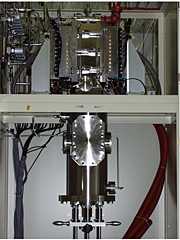
Cross-sectional electron micrograph of a sandwich structure with an extremely thin nanometric oxide film
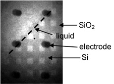
Near infrared transmission image of a nano-gap device filled with liquid
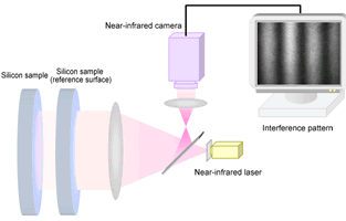
Near infrared measurement on a flat silicon surface
Silicon is used for such purposes as semiconductor device substrates and mirrors for synchrotron radiation due to its excellent crystal properties. However, these applications require a high dimensional accuracy, and thus, we are developing a measurement method to measure a single crystal silicon flat surface. We have created a near infrared interferometer at a wavelength where silicon is transparent, 1.3 µm. Among the three samples, the phase shifting interferometry is measured three times (three-flat method) on three different pairs of samples, which yield an absolute flatness measurement on all three samples with an accuracy that is even higher than the reference surface.
Device process evaluation by nanoscale surface measurements
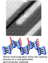
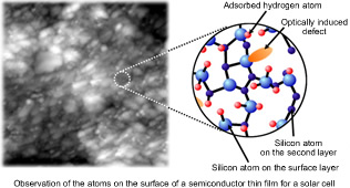
To realize high performances of electronic and optical devices, it is essential to measure and evaluate the surface fabrication processes and thin film fabrication processes at the atomic level, and then optimize them. In case of semiconductor devices, for instance, their substrates should have their atomic level roughness (micro-roughness) reduced to the theoretical limit by controlling the wet cleaning process of silicon wafers. To achieve superior quality solar cells, a thin film fabrication technology must be developed that realizes a high efficiency in the entire region of the active layer where photoelectric conversion occurs. Our laboratory is working on developing and applying surface nanoscale measurement technologies in order to improve the performance of device processes. To date, we have succeeded in the local visualization of the photoelectric conversion efficiency distribution on an amorphous thin film surface for solar cells, and in the evaluation of the atomic structure on a semiconductor substrate surface after the wet cleaning process and ultra-precision machining process. We have also begun to develop a new material evaluation method where information on bulk material is reflected on its surface.
565-0871, Japan
Department of Precision Science & Technology, Osaka University
E-mail:
www_admin[at]prec.eng.osaka-u.ac.jp