Research Center for Ultra-Precision Science & Technology
(Endo Laboratory)
|
Jump to Research Center for Ultra-Precision Science & Technology |
“Developing innovative surface creation technology”
Frontier industry and fundamental science in the 21st century require “manufacturing” with atomic-level accuracy. Our central purpose of research is the continuous development of original technology in “atomistic production engineering” where fundamental physics and chemical phenomena utilized in engineering processes such as ultra-precision machining, thin film growth, and microfabrication should be analyzed and elucidated from the atomistic and electrical viewpoints. Targets of the center are to develop an original novel manufacturing process apparatus based on the “atomistic production engineering”, to manufacture useful “products” by the newly developed apparatus, and to evaluate the performance of the products. By doing so, the center plays a role in bringing up practical technologies fruitful in the human society from seeds in the university.
Ultra precision shape creation group
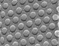
In order to manufacture ultra precision optical components and to process functional materials, figures must be created on the nanometer level with a high degree of reproducibility, but without introducing surface damages. The novel processing technologies that our group is proposing, called the plasma chemical phase vaporization machining (PCVM) utilizing atmospheric pressure plasma and the local wet etching (LWE), are non-contact chemical processes without mechanical load to the workpiece. Therefore, in these processes, the removal function and removal rate are insensitive against the external disturbances, such as vibration and thermal deformation of the machine and the workpiece, and damaged layer is not induced in the removal process. In addition, these technologies are able to accurately control the amount of surface material to be processed with nanometer level precision by controlling the welling time of the plasma or etchant. We are currently applying these technologies to manufacture X-ray focusing mirrors, neutron mirrors, SOI wafers, quartz crystal wafers, and large sized photo masks for next generation liquid crystal displays.
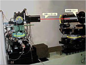
Aspherical surface ultra-precision measurement group
In general, laser interferometer is used for precision figure measurement, but measurable figures are limited because relative shape difference with the reference plane, and absolute measurement accuracy is strongly dependent on accuracy of the reference plane. In our measuring system, angle of light source and the sample are adjusted so that incident laser beam on the sample may overlap with reflection laser beam, and the ray vector is coinciding with the normal vector. And by measuring the angle in which light source and sample moved using the ultra-high accuracy goniometer, the angle in which light source and sample moved using the ultra-high accuracy goniometer, the value of normal vector is obtained at the absolute accuracy over 5 x 10⁻⁸ rad (targeted value). Then it is possible to construct the shape of the free curved surface at the accuracy of the nano meter level by integrated normal vector in the each point on the mirror plane similarly required. This measurement principle was proposed and verified by cooperative research with high energy accelerator research organization (KEK, Tsukuba Japan). This measuring method is seldom influence from disturbance such as refractive index fluctuation, because this method is the common path type in which the path of incident light and reflected light are same. And it is possible to measure various ashperical shapes in the absolute accuracy of 1nm p-v.
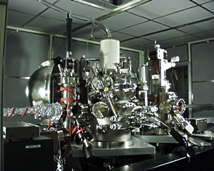
Surface atomic structure and function measurement group
Ultimate measuring technologies based on novel concept are developing for evaluating function od surface, thin film, fine structure those are fabricated by ultra-precision machining and thin film formation process. And elementary reaction processes on the surface in above fabrication processes are clarified by observation of atomic and electronic state using surface science technique.
Surface functionalization group
Based on the diversity in a chamber-less atmospheric plasma processing coupled with nanometer order self organizational processing, our group is developing an environmentally-friendly high precision functional surface creation technology. There are six advantages to our method: (1) It is easy to manufacture a large-sized substrate. (2) Few processes are involved. (3) High resolution is possible. (4) Only small amounts of waste materials are produced, of which very little are hazardous substances, and all are easy to collect. (5) Our method requires a small investment in facilities and little processing equipment. And (6) our method can be transferred from a clean room to a clean booth. In addition to these advantages, this novel highly functional surface creation technology can add a very wide range of functionalities to one piece of equipment by only changing the type of supplied gas, polymers, or metals. Hence, our method lends itself to a wide range of industrial applications. We are currently considering its applications to thickness adjustment processing of AT-cut quartz wafers, and catalyst-free electroless copper deposition.
Nano-structure creation group
Nano-particles are the most fundamental structural elements to form nano-structures, and they are the smallest structures to retain the properties of molecules and atoms. They have been synthesized in various material systems such as semiconductors and metals. Moreover, it is highly anticipated that nano-particles will be applied to electronics and biotechnologies. Our group will expand the precision boundaries of synthetic technologies and the arrangement of nano-particles by utilizing ultra-precision processing technologies. In addition, we will conduct application research on material systems suitable for device applications, which will thereby accelerate the commercial application of nano-technology products. Furthermore, we are currently developing initiatives in nano-particle optical contrast agents, near infrared responsible localized surface plasmon resonance sensors, and a precious nanometer scale assembly process for nano-particle devices.
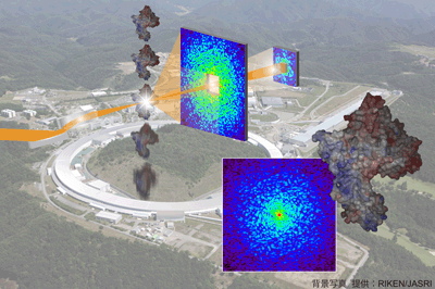
Development and Application of Coherent X-ray Diffractive Imaging
The discovery of X-ray diffraction from crystals by Max von Laue nearly a century ago opened a new era for visualizing the arrangement of atoms in three dimensions. Indeed, X-ray crystallography has made revolutionary impacts in physics, chemistry, materials sciences, biology and medicine, and a number of Nobel prizes have been awarded in this field. X-ray crystallography can determine almost any structure, as long as good-quality crystals are obtained. However, many samples such as quantum dots, nanowires, cells, organelles, and viruses, cannot be accessed by this approach. To overcome this limitation, the employment of different techniques and methods is required. One promising approach is coherent diffraction microscopy. In principle, diffraction microscopy can observe non-crystalline sample with atomic resolution. Single-shot imaging of single molecules will be realized by using X-ray free electron lasers, which are the next-generation light source. Coherent x-ray imaging group develops the x-ray diffraction microscopy and carry out application studies in biological and materials sciences
[Keyword]
Coherent x-ray optics, Phase retrieval calculation, Synchrotron radiation, X-ray free electron laser
565-0871, Japan
Department of Precision Science & Technology, Osaka University
E-mail:
www_admin[at]prec.eng.osaka-u.ac.jp