
Atomically Controlled Processes Laboratory (Kuwahara Laboratory)
|
“To view and manipulate the atomic and molecular world”
It has become possible to actually view, touch, and move atoms and molecules in the nanometer world, thanks to advances in science and technology. Today we can assemble atoms and molecules to construct synthetic nanometric structures, which do not exist in nature. In such a microscopic world, we expect to discover various special physical phenomena, states of electrons, electron transport properties, and quantum effects, which are currently unknown.
Our laboratory is developing new equipment to precisely measure minute physical and chemical quantities of atoms and molecules. Based on the knowledge gained through these measurements, we are developing novel devices that work on new concepts, thereby contributing to the ultimate “product realization” using atoms and molecules. We consider the synthetic creation of novel nano-materials an important innovation frontier for the future of an advanced information society.
Photon STM group
Tunneling current-induced luminescence analysis is a nano-physical evaluation method to analyze photo luminescence from the nanoscale regions on an atomic and molecular level, which is induced by the tunneling current of STM. This analysis method enables to capture the luminescence from nanometric regions, which cannot be measured by conventional optical methods. Our laboratory is conducting research in projects such as (1) analysis of the luminescence properties of nanometric structures, including carbon nanotubes, which are anticipated for use in future optical devices, and (2) analysis of charge injection phenomena at interfaces of organic thin film devices, which will become critical in their operation, by capturing luminescence from the organic thin films.
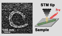
<Figure 1>
Synchrotron radiation STM group
Synchrotron radiation (SR) is highly intense light (especially in X-ray region) with a wide range of wavelengths, which is generated from accelerated charged particles. Our group is evaluating the properties and functions of materials at the atomic level using STM combined with SR as a probe. We perform our experiments at SPring-8 (SR facility). We have developed a unique system to observe the interactions between high intensity SR and materials on the nanometric scale in real space. We have successfully identified elements on a Ge nano-island fabricated on a Si(111)7X7 surface with a spatial resolution of a few nm. Currently, we are performing measurements and evaluations on various surfaces using this system.
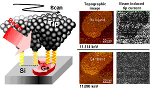
<Figure 2>
Independently driven two-probe STM group
Our group is developing in-house local electrical conduction measurement equipment using two STM probes, which are independently driven. Our current emphasis is on electrical conduction property measurements at atmospheric pressure and room temperature. We have successfully measured conductivity in the nanometer to several micrometer regions, which is not possible with conventional measurement methods. To date, we have successfully obtained the highest conductivity in a one-dimensional electrical conduction measurement on a polydiacetylene molecule thin film. In addition, we have visualized the local electrical conduction on a two–dimensional uniform conductive thin film.
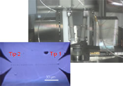
<Figure 3>
Organic and molecular device group
Our group is conducting research that employs the so-called nano-gap electrodes, which are microscopic electrodes with about 100 nm intervals on an insulating substrate. Current projects include (1) electrical measurements on conductive organic molecules and (2) development of molecular devices using a new concept that employs these conductive organic molecules. Moreover, we are fabricating nano-gap flat electrodes without steps on the surface on a molecular order. These flat electrodes have characteristics of being able to place molecules between electrodes while effectively using bottom-up processes such as self organization because the molecules’ own structures remain intact. By placing various organic thin films and single crystals on these electrodes, we are developing never-before-realized nanometric molecular devices with short channels.
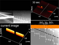
<Figure 4>
CAICISS group
CAICISS (CoAxial Impact-Collision Ion Scattering Spectroscopy) group is conducting research in fabricating atomic scale flat ferroelectric surfaces, and analyzing their structures (in particular, LiNbO3 and LiTaO3, which are widely used for SAW device substrate, and optical or piezoelectric devices). We have been successful in ultra flattening these surfaces using a simple method. Furthermore, by analyzing the angular dependence of the intensity of particles (low energy ion) scattered on these surfaces, we can determine the structure of the region near the surface in the atomic layer level (CAICISS). This information is useful for controlling the growth of the electrodes on the substrate surface and also serves for developing high density memories.
Structural color group
Color, which is generated without pigment and is due to interaction between the microscopic structure of a material and light, is called “structural color.” A typical example of structural color can be seen on wings of a Morpho butterfly (left figure) from South America, which is called a “living jewel” and commonly appears on TV commercials. The mystery of the beautiful color, however, is that it appears blue from wide range of angles, instead of being rainbow colored, despite the fact that this is an interference color. For a long time, this phenomenon has attracted the attention of many researchers. The key to understanding this color is the nanometric structure on the surface. Thus, we aim to analyze this mechanism in order to reproduce the Morpho butterfly color using an engineering method, and to further to apply this method to various industries to appeal to visual pleasures.
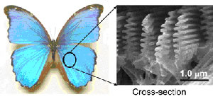
<Figure 5>
565-0871, Japan
Department of Precision Science & Technology, Osaka University
E-mail:
www_admin[at]prec.eng.osaka-u.ac.jp