Ultra-Precision Machining Laboratory (Yamauchi Laboratory)
|
Jump to Ultra-Precision Machining Laboratory  |
“Create what could not be created”
To “create what could not be created” is the first step in the progress of science and technology. Our laboratory is tackling giant-scale nanotechnology where the structure is controlled on an atomic scale over a large area spanning several 100 mm. In recent years, we have developed nano-machining and nano-measurement systems such as EEM, PCVM, MSI, RADSI, UPW-ECM, and CARE. Using these systems, we have succeeded in “creating what could not be created” such as high performance electronic and optical device substrates, X-ray devices, and X-ray nanoscopes. Furthermore, we are contributing to pioneering new science and technology in collaboration with a variety of fields such as biology, medical science, drug discovery, semiconductor devices, and X-ray free electron lasers. Our motto in education is a “multi-major education” where training in sub-majors through collaborative research is emphasized in addition to the main specialty of ultra-precision machining and measurement systems with an extensive use of surface science.
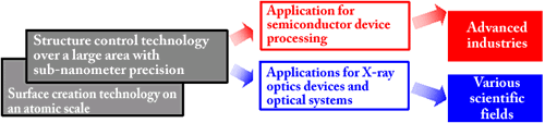
Atomistic production technology
Frontier science and technology in the fields such as surface science, semiconductor and optics, often require extremely smooth surfaces on an atomic level. Our laboratory is conducting fundamental researches, regarding on new surface smoothing and figuring technology by investigating and applying various physical and chemical phenomena, in which surfaces are smoothed naturally on an atomic level.
[Keywords]
EEM (Elastic emission machining), PCVM (Plasma chemical vaporization machining), electrolytic machining in ultrapure water, CAtalyst-Referred Etching (CARE), and numerically controlled sacrificial oxidation method
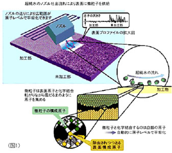
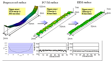
<Figure 2> Atomistic planarization by EEM
Giant-scale nanotechnology
Optical elements such as mirrors and lenses used in advanced optical instruments, acutely require technologies to make flat, spherical and non-spherical shapes with sub-nanometric precision in the upward direction, while covering a large surface area of 10 to 100 mm in the planer direction. Our laboratory is working on developing surface figuring systems on the basis of the computer-control, in which the measured profiles are turned into ideal ones. In our group, not only machining but also figure measurements with stitching interferometry have been researched. By combining these interferometric measurement methods and the new production methods mentioned above, we can gain the ability to obtain a large area surface with subnanometric precision.
[Keyword]
Large area microstitching interferometry, RADSI (Relative Angle Determinable Stitching Interferometry), and large scale nano-precision copying process
Application to semiconductor device processing
There are numerous considerations when applying laboratory technologies to commercial industries such as manufacturing costs, manufacturing speed, and environmental impact as well as performance. Our laboratory is considering these points and conducting research to apply the above-mentioned technologies to manufacture substrates for semiconductor devices. We have already successfully developed technologies to manufacture SiC substrates and SOI substrates, which have the world’s best performances and are receiving attention from different industries.
[Keyword]
Ultra thin silicon film, next generation electronic devices, electrolytic machining in ultrapure water, copper damascene interconnect processes, high performance dry process in wide bandgap semiconductor substrate manufacturing, and planarization of SiC and GaN single crystal wafers
X-ray optics and optical system
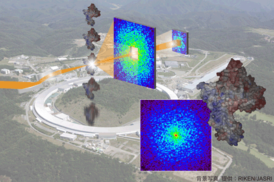
Leveraging on our technology to control a structure over a large area with subnanometric precision, we have successfully fabricated hard X-ray focusing mirrors with a focused beam size less than 30 nm, which is the smallest in the world. These devices allowed us to actualize an X-ray microscopy system having a nanometer level spatial resolution. We are currently working with the optics group of SPring-8 (RIKEN) to: (1) realize sub 10nm X-ray nm focusing, (2) develop an ultra-high resolution scanning X-ray microscope, and (3) develop a coherent X-ray diffraction microscope.
[Keyword]
Imaging optics system for extreme ultraviolet light lithography, hard X-ray focusing mirror, multi-layer X-ray mirror, ultra high resolution scanning X-ray microscope, ultra high resolution X-ray micro CT, and coherent diffraction microscope
Development and Application of Coherent X-ray Diffractive Imaging
The discovery of X-ray diffraction from crystals by Max von Laue nearly a century ago opened a new era for visualizing the arrangement of atoms in three dimensions. Indeed, X-ray crystallography has made revolutionary impacts in physics, chemistry, materials sciences, biology and medicine, and a number of Nobel prizes have been awarded in this field. X-ray crystallography can determine almost any structure, as long as good-quality crystals are obtained. However, many samples such as quantum dots, nanowires, cells, organelles, and viruses, cannot be accessed by this approach. To overcome this limitation, the employment of different techniques and methods is required. One promising approach is coherent diffraction microscopy. In principle, diffraction microscopy can observe non-crystalline sample with atomic resolution. Single-shot imaging of single molecules will be realized by using X-ray free electron lasers, which are the next-generation light source. Coherent x-ray imaging group develops the x-ray diffraction microscopy and carry out application studies in biological and materials sciences
[Keyword]
Coherent x-ray optics, Phase retrieval calculation, Synchrotron radiation, X-ray free electron laser
565-0871, Japan
Department of Precision Science & Technology, Osaka University
E-mail:
www_admin[at]prec.eng.osaka-u.ac.jp