Applied Surface Science Laboratory (Watanabe Laboratory)
|
“Development of new materials and new processes for the broadband and mobile age”
As Internet access has become more and more common, information from anywhere in the world can be obtained from the comfort of our own home. Nowadays, society is moving towards the age of broadband connection. “Broadband” in the internet means “wide road”. Hence, broadband will make roads, which connect your home and cellular phones to the world, several-thousand times wider. In the near future, you may be able to telecommute, or even receive medical care at home without visiting a hospital. In order to realize such a society, electronic devices that are much faster and consume much less power must be developed. Our laboratory aims to develop and evaluate new electronic materials and processes as part of this movement. For instance, an advanced LSI contains several hundred millions of semiconductor devices within a square, which has a side of several millimeters, and the size of each individual device within an LSI is measured in nanometers. Hence, we not only need to precisely control their fabrication processes, but also design the characteristics of the electrodes and substrate materials in order to improve the performance of these devices. Therefore, we are conducting research from a wide range of viewpoints, but our emphasis is on deepening the understanding of the atomic world in order to support the next-generation electronics industry.
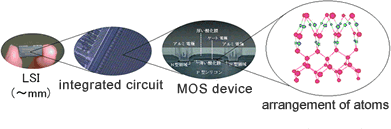
<Figure 1> Semiconductor devices in LSI
Research and development on semiconductor devices to realize
high-speed, low-power consumption LSIs
As semiconductor devices scaled down to nanometer regime, the quantum effects become an increasingly important limitation on device performance. In particular, a silicon dioxide film, which is used as a gate insulator of MOS devices, has been thinned down to 1 nm, and the leakage current due to the quantum tunneling effect is currently a major hurdle. To overcome this issue, our laboratory is working on the research and development of materials, structures, and process technologies of a high dielectric constant gate insulator and metal gate electrode, which can provide high drive current without increasing the leakage current. In addition, our research encompasses the realization of devices fabricated on a germanium substrate instead of a silicon substrate, which is currently used as the LSI substrate, due to the superior carrier mobility of germanium. Our studies include: (1) Ge surface cleaning techniques, (2) dielectric film fabrication technology on Ge as well as (3) fabrication and characterization techniques of SGOI (SiGe On Insulator) and GOI (Germanium On Insulator) wafers, which are next-generation semiconductor substrates.
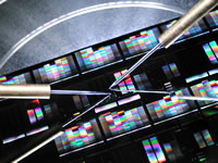 <Figure 2> Electrical characterization of fabricated devices |
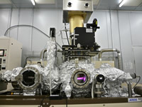 <Figure 3> Surface processing / dielectric film formation equipment |
Ideal surface and dielectric film formation technology on wide bandgap semiconductors
Wide bandgap semiconductors such as silicon carbide (SiC) are attracting much attention as semiconductor device materials for power devices to drive the motors of Shinkansen (bullet trains) and hybrid cars, and to transport electrical energy with high efficiency. Silicon (Si) is currently a mainstream material, but employing a wide bandgap material is expected to reduce power consumption as well as carbon dioxide emission. In order to make the best use of the superior properties of wide bandgap materials, new technologies are needed to prepare an ideal surface and to improve the interface characteristics between dielectric films. Our laboratory is developing new processes using high density plasma and exploring new materials in order to realize SiC power devices.
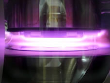
<Figure 4>High density plasma
Use of synchrotron radiation and its application to electronics
Synchrotron radiation has been called dream light in the 21st century. We are evaluating the physical properties of electronic materials at the atomic level using this dream light. We are carrying out measurements with the utmost precision on new materials and next generation semiconductor substrates at the synchrotron radiation facilities of SPring-8 (with a huge electron accumulation ring with a 1,400 m circumference) located at Harima Science Garden City, and the Photon Factory at High Energy Accelerator Research Organization (KEK) at Tsukuba.
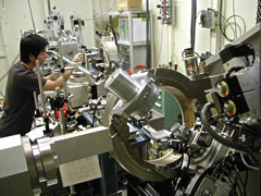
<Figure 5> Synchrotron radiation experiment at SPring-8
565-0871, Japan
Department of Precision Science & Technology, Osaka University
E-mail:
www_admin[at]prec.eng.osaka-u.ac.jp