Laboratories
 Functional Materials Area
Prof. Hiromasa Ohmi Assoc. Prof. Hiroaki Kakiuchi 【】Functional materials, Plasma, Solar cells, Thin film transistors, Diamond synthesisIn our laboratory, basic and application studies have been carried out, regarding novel surface creation processes such as Elastic Emission Machining (EEM), Plasma Chemical Vaporization Machining (PCVM), and Catalyst Referred Etching (CARE), for flattening advanced material surfaces or fabricating ultraprecise X-ray optics. Since their process mechanisms are on chemical reaction basis, high quality surfaces with no mechanical damage can be produced. For example, targets of applications are X-ray mirror, EUV mirror, SOI wafer, and SiC/GaN substrate. By using fabricated X-ray mirrors, X-ray nanobeam systems and various X-ray microscopes has been successfully developed for various scientific fields such as biology, medical science, nanotechnology and material science.
 Arima Lab. | Nano Surface and Interface Engineering Area
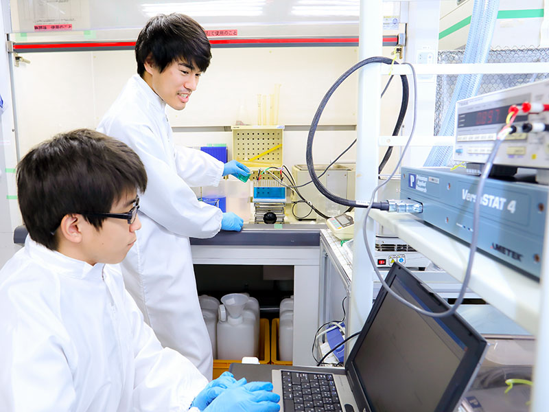
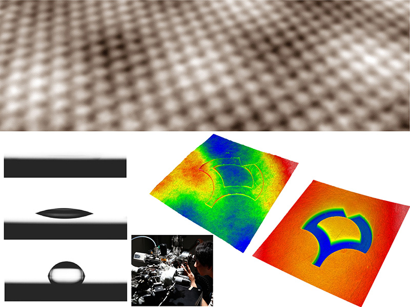
Prof. Kenta Arima Assis. Prof. Kouji Inagaki 【】Semiconductor surface, Solid/liquid interface, surface science, NanomaterialIn order to realize manufacturing technology with extreme precision, it is essential to understand the interactions between solid-liquid and solid-gas interfaces at the atomic and molecular level and to control them based on science. Our laboratory conducts research on ultra-precise surface measurement using microscopes that can visualize atomic arrangements, spectroscopic analysis that is sensitive to a few atomic layers on the surface, and high-precision simulations based on quantum mechanics. We also aim at creating high-performance semiconductor nanomaterials by novel etching phenomena and developing new surface processes. Through these efforts, we would like to contribute to the dramatic sophistication of production technology and the realization of a clean and comfortable energy-using society.
 Ogi Lab. | Quantum Measurement and Instrumentation Area
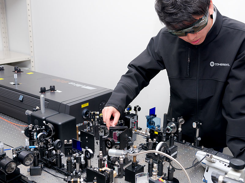
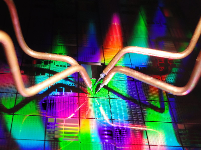
Prof. Hirotsugu Ogi Assoc. Prof. Kichitaro Nakajima Assis. Prof. Yasushi Oshikane Assis. Prof. Natsumi Fujiwara 【】Ultrasonics, fs-pulse laser, Biosensors, Alzheimer's disease, Smart phone, SpintronicsUsing our original optical-acoustical measurement systems, we study mechanical behavior of nanomaterials and kinetics of biomolecules, and develop instruments for diagnosis and drug discovery. One important keyword is “resonance”. At resonance, information on mechanical and electromagnetical properties are highly enhanced, allowing high-sensitive measurements in material-biological science. We control sound via light and vice versa to investigate thermodynamic properties in nanofilms, nanowires, and nanodots, and binding and aggregation reactions among various biomolecules. We also study application of our original phonon-photon measurements for biosensors and diagnosis for neurodegenerative diseases, including Alzheimer's disease.
 Atomically Controlled Processes Area
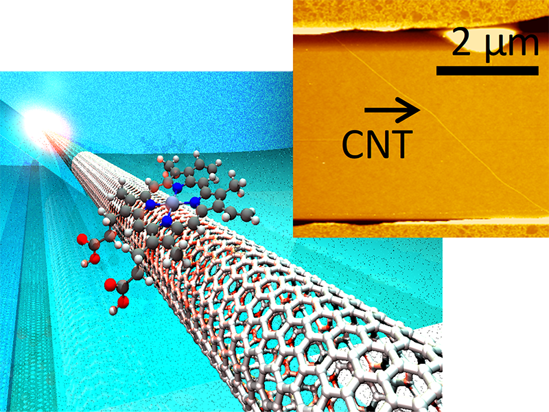
Assoc. Prof. Akira Saito Assis. Prof. Takuma Hattori 【】Nanotechnology, Suruface Science, NanodeviceIt has become possible to actually view, touch, and move atoms and molecules in the nanometer world, thanks to advances in science and technology. Today we can assemble atoms and molecules to construct synthetic nanometric structures, which do not exist in nature. In such a microscopic world, we expect to discover various special physical phenomena, states of electrons, electron transport properties, and quantum effects, which are currently unknown. Our laboratory is developing new equipment to precisely measure minute physical and chemical quantities of atoms and molecules. Based on the knowledge gained through these measurements, we are developing novel devices that work on new concepts, thereby contributing to the ultimate “product realization” using atoms and molecules. We consider the synthetic creation of novel nano-materials an important innovation frontier for the future of an advanced information society.
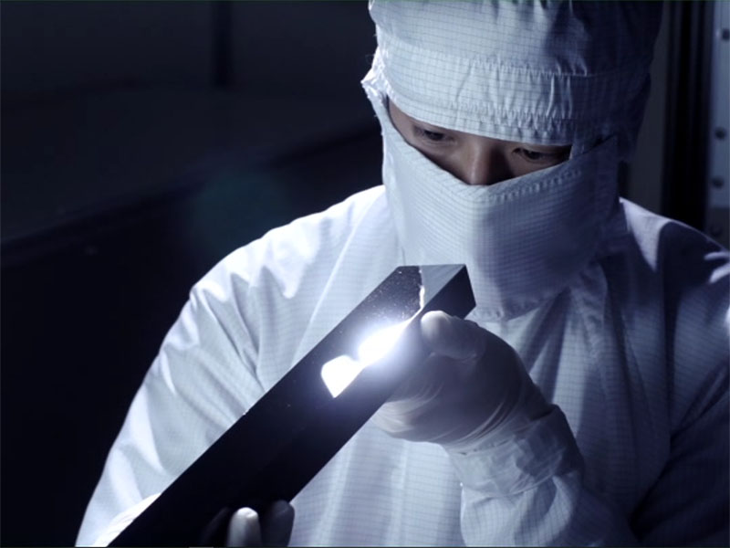 Sano Lab. | Ultraprecision Machining Area
Prof. Yasuhisa Sano Assoc. Prof. Junpei Yamada Assis. Prof. Daisetsu Toh 【】EEM, CVM, CARE, X-ray mirror and microscope, split-and-delay optics, atomic-scale surface creation, SPring-8, SACLAIn our laboratory, basic and application studies have been carried out, regarding novel surface creation processes such as Elastic Emission Machining (EEM), Plasma Chemical Vaporization Machining (PCVM), and Catalyst Referred Etching (CARE), for flattening advanced material surfaces or fabricating ultraprecise X-ray optics. Since their process mechanisms are on chemical reaction basis, high quality surfaces with no mechanical damage can be produced. For example, targets of applications are X-ray mirror, EUV mirror, SOI wafer, and SiC/GaN substrate. By using fabricated X-ray mirrors, X-ray nanobeam systems and various X-ray microscopes has been successfully developed for various scientific fields such as biology, medical science, nanotechnology and material science.
 Morikawa Lab. | Computational Physics Area
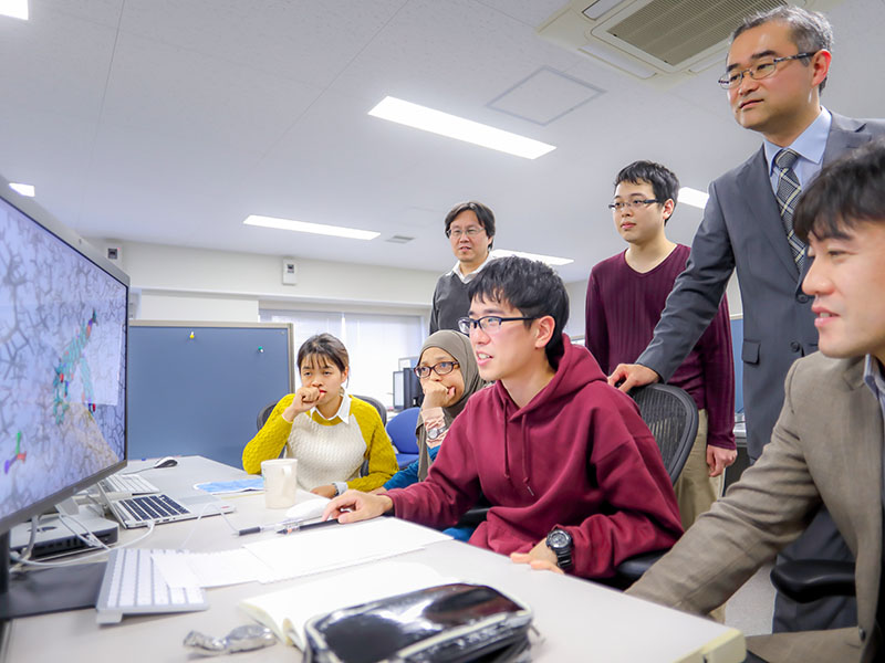
Prof. Yoshitada Morikawa Prof. Ikutaro Hamada Assis. Prof. Harry H. Halim 【】CMD, First-principles, DFT, Simulation, Electronic Structure, Solid State Physics, Surface Science, Catalysis, Organic DevicesTo develop highly functionalized materials for various applications such as electronic devices, solar cells, highly efficient fuel cells, organic devices, and so on,it is important to clarify behaviors of electrons and atoms in materals in detail. However, it is often difficult to elucidate such microscopic phenomena experimentally. To this end, we employ first-principles computer simulations and observe electrons and atoms in atomic scale and predict properties of new materials. We develop computer simulation programs based on ""Quantum Mechanics"" and by using those programs on super computers, we investigate physical and chemical properties of materials and clarify the origins for those properties. Based on these investigations, we propose important factors to desing new efficient materials and contribute to fields related to industry, energy and enviroment which are important in fugure of our society.
 Watanabe Lab. | Advanced Device Engineering Area
Prof. Heiji Watanabe Assoc. Prof. Takuma Kobayashi Assis. Prof. Masahiro Hara Assis. Prof. Akihiro Takeuchi Technician Mikito Nozaki 【】Semiconductor, Nanoelectronics, Power device, X-ray imagingHumanity is confronted with many global-scale issues that include depletion of fossil energy and other natural resources, food shortage and population explosion, climate change and natural disaster, and urban development and poverty. Technology has the potential for significant impact to overcome these challenges and build a sustainable society. In response to the hopes, dreams, and wishes that people find through family, friends, and community, we believe that science and technology should be developed to enable humanity to responsibly coexist and thrive with nature in environmental harmony. To realize a sustainable and prosperous future, we aim to facilitate technological innovation by designing new materials, combining dissimilar materials, and introducing new structures with wide-range of capabilities contributing to next-generation of green nanoelectronics.
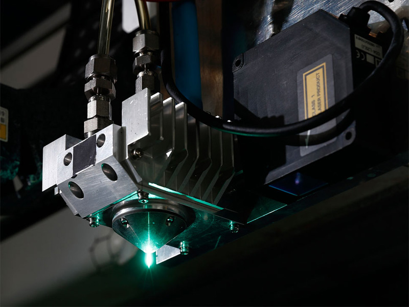 Yamamura Lab. | nanoManufacturing Science Area
Prof. Kazuya Yamamura Assoc. Prof. Yuji Ohkubo Assis. Prof. Rongyan SUN 【】Plasma-assisted nano-precision processing, electrochemical processing, surface and interface functionalization, wide-gap semiconductor substrates, diamond substrates, fluoropolymer surface modificationSince the dawn of history, civilization has evolved with persistent efforts to develop manufacturing technologies. In this research area, we are creating novel innovative manufacturing technologies to manufacture state-of-the-art optical elements, semiconductor substrates, and highly functionalized substrates that require nano- and sub-nanometer order accuracy. Under the philosophy that new technology created by us triggers a new industrial revolution in the 21st century and contributes to the further development of mankind, we are immersed in the research and development of “nanoManufacturing process” that having both extreme precision and efficiency.
